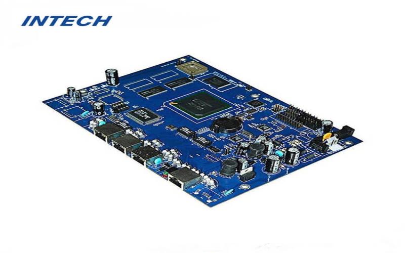
Common PCB layout principles
Date:2023-06-08 14:56:30
一. According to the principle of signal direction layout
1. Usually, the position of each functional circuit unit is arranged one by one according to the signal flow, and the core component of each functional circuit is the center, and the layout is carried out around it.
2. The layout of the components should facilitate the flow of signals, so that the signals can be kept in the same direction as possible. In most cases, the flow direction of the signal is arranged from left to right or from top to bottom, and the components directly connected to the input and output terminals should be placed close to the input and output connectors or connectors.

二. Component arrangement rules
1. Under normal conditions, all components should be arranged on the same surface of the printed circuit. Only when the top layer components are too dense, can some devices with limited height and low heat generation, such as chip resistors and chip capacitors , Paste IC, etc. on the bottom layer.
2. Under the premise of ensuring electrical performance, the components should be placed on the grid and arranged parallel or vertically to each other in order to be neat and beautiful. Generally, components are not allowed to overlap; the components should be arranged compactly, and the input and output components should be kept as far away as possible.
3. Components with high voltage should be arranged in places that are not easily accessible by hand during debugging.
4. Components located on the edge of the board are at least 2 board thicknesses away from the edge of the board.
5. There may be a high potential difference between certain components or wires, and the distance between them should be increased to avoid accidental short circuits due to discharge and breakdown.
6. Components should be evenly distributed and densely distributed on the entire board.

