 English
Classification of holes on PCB and their functions
Date:2023-09-26 11:39:53
Holes on PCB are divided into plated holes (PTH) and non-plated holes (NPTH) according to whether they participate in electrical connections.
Plated holes (PTH) refer to holes whose walls are plated with metal, which can achieve electrical connections between the inner and outer layers of the PCB or the conductive patterns on the inner and outer layers. Its size is determined by the size of the drill hole and the thickness of the plated metal layer. Non-plated holes (NPTH) are holes that do not participate in the electrical connection of the PCB, that is, non-metallized holes. According to the level of holes penetrating the inner and outer layers of PCB, holes can be divided into through holes, buried holes and blind holes.
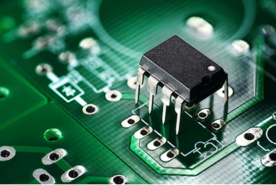
Through holes run through the entire PCB and can be used to achieve inner layer connections and/or positioning and installation of components. Among them, the holes used for fixing component terminals (including pins and wires) to the PCB and/or achieving electrical connection are called component holes. Plated holes that are used for inner layer connections but do not contain component leads or other reinforcing materials are called via holes. There are two main purposes of drilling through holes on the PCB: one is to create an opening through the board, allowing subsequent processes to form electrical connections between the top, bottom and inner layers of the board; the other is to enable the installation of components on the board Maintain structural integrity and positional accuracy. Blind vias and buried vias are widely used in high-density interconnection HDI. Blind vias typically connect layer 1 to layer 2. In some designs, blind vias can connect layer 1 to layer 3. Combining blind and buried vias enables more connections and higher board density required for HDI. This enables increased layer density in devices with smaller pitches while also increasing transmission power. Hidden vias help keep the board lightweight and compact. Blind and buried via designs are common in complex, lightweight, higher-cost electronic products such as mobile phones, tablets, and medical devices. Blind holes are formed by controlled drilling depth or laser ablation. The latter is the more common method currently used. The stack of vias is formed by sequential lamination. The resulting vias can be stacked or staggered, adding extra steps to manufacturing and testing while also increasing cost. According to the purpose and function of the hole, it is divided into: Via (via) is a metallized hole that realizes the electrical interconnection between different conductive layers on the PCB. It is not used for plugging components.
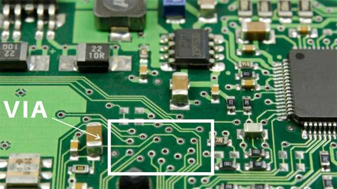
PS: The via holes here are based on the levels above that penetrate the inner and outer layers of the PCB. The via holes can be subdivided into through holes, buried holes and blind holes. Component holes are holes used for welding and fixing plug-in electronic components and connectors. They are usually metallized holes. They can also serve as electrical interconnections between different conductive layers.
Mounting hole: A hole with a larger diameter on the PCB, used to fix the PCB to a carrier such as a housing.
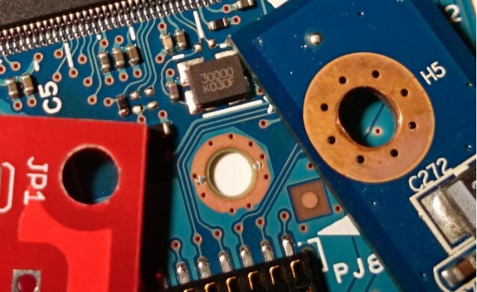
Slots are automatically converted into a collection of multiple single holes in the drilling program of the drilling machine or slots processed by milling. They are generally used as installation pins for connector devices, such as oval pins for sockets.
