What are the Key Steps in Electronics PCB Manufacturing?
Date:2023-12-13 15:15:32
Printed Circuit Board (PCB) manufacturing is a critical step in the production of electronic devices. PCBs are the backbone of these devices, connecting various components and enabling them to function cohesively. This article will provide comprehensive insights into the key steps involved in the PCB manufacturing process, ensuring a clear understanding of this complex procedure.

Step 1: Designing the PCB
The first step in the PCB manufacturing process is to design the circuit board using computer-aided design (CAD) software. Designers create a blueprint of the PCB, including the placement of components, routing traces, and defining layers. This crucial step ensures the proper functioning and durability of the final product.
Step 2: Fabricating the Inner Layers
Once the design is finalized, the manufacturing process begins with the fabrication of the inner layers. This involves selecting the substrate material and applying a layer of copper to both sides. A photosensitive material called a resist is then applied, which is hardened using ultraviolet light through a photomask, leaving behind the desired copper traces.
Step 3: Aligning and Bonding Layers
After fabricating the inner layers, they are aligned, stacked, and bonded together to form a multi-layered PCB. The alignment is crucial to ensure that the copper traces on each layer align correctly. A combination of heat and pressure is then applied to bond the layers, creating a solid structure for the PCB.
Step 4: Drilling and Plating
After bonding, precision holes are drilled into the PCB at specific locations to accommodate component leads and allow for electrical connections. These holes are then plated with a thin layer of copper, enhancing their conductivity and preventing corrosion. The plating process also enhances the durability of the PCB.

Step 5: Applying Solder Mask and Silk Screen
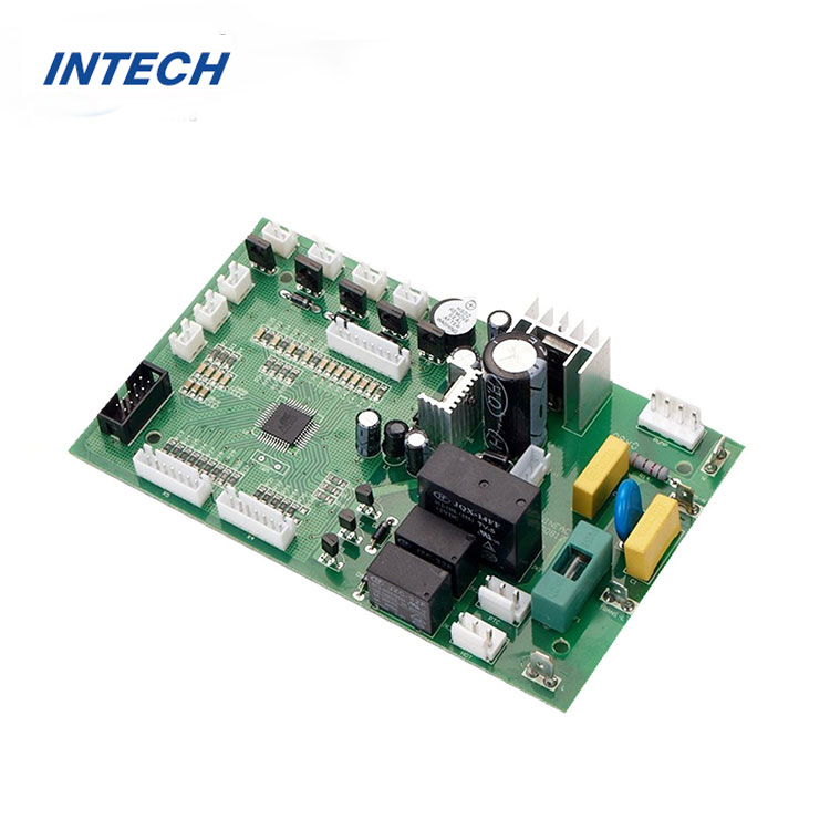
To prevent unwanted electrical connections and protect the copper traces, a solder mask is applied to the surface of the PCB. This solder mask is typically green in color and covers all areas except where the components will be soldered. Additionally, a silk screen layer is added, which displays component names, reference numbers, and other details.
Step 6: Component Assembly
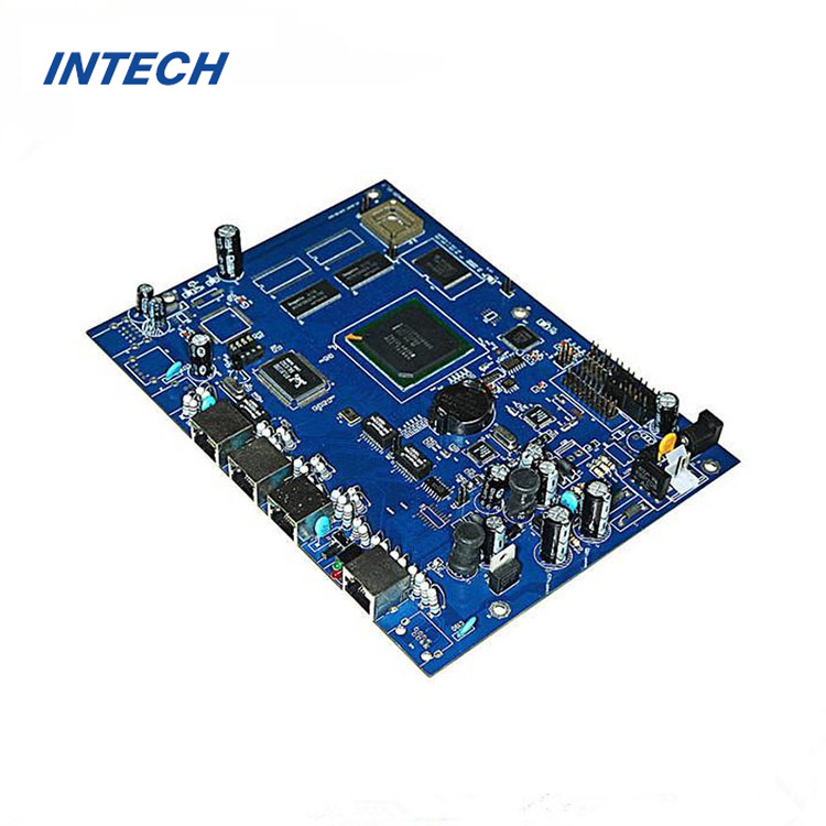
In this step, electronic components such as resistors, capacitors, and integrated circuits are soldered onto the PCB. Advanced manufacturing processes, such as surface mount technology (SMT), are used to place components on the board accurately. Careful attention is given to ensure proper orientation, precise soldering, and adherence to industry standards.
Step 7: Testing and Quality Assurance
After component assembly, the PCB undergoes rigorous testing and quality assurance procedures. This includes electrical testing to verify the functionality of the circuit, as well as visual inspections to check for any manufacturing defects or soldering issues. Quality control measures ensure that only reliable and defect-free PCBs are sent for final production.
Step 8: Final Production and Packaging
Once the PCB passes all tests and quality checks, it is ready for final production. This involves integrating the PCB into the electronic device, connecting it with other components, and performing additional testing to ensure its compatibility and overall functionality. The finalized PCB is then packaged appropriately, ready for distribution to end-users.
Summarizing the PCB Manufacturing Process
PCB manufacturing involves a series of intricate steps, starting from the initial design phase to the final production and packaging. Each step demands precision, attention to detail, and adherence to industry standards to ensure a reliable and high-quality end product. By understanding the key steps involved in the PCB manufacturing process, one can appreciate the complexity and significance of this crucial stage in electronic device production.
