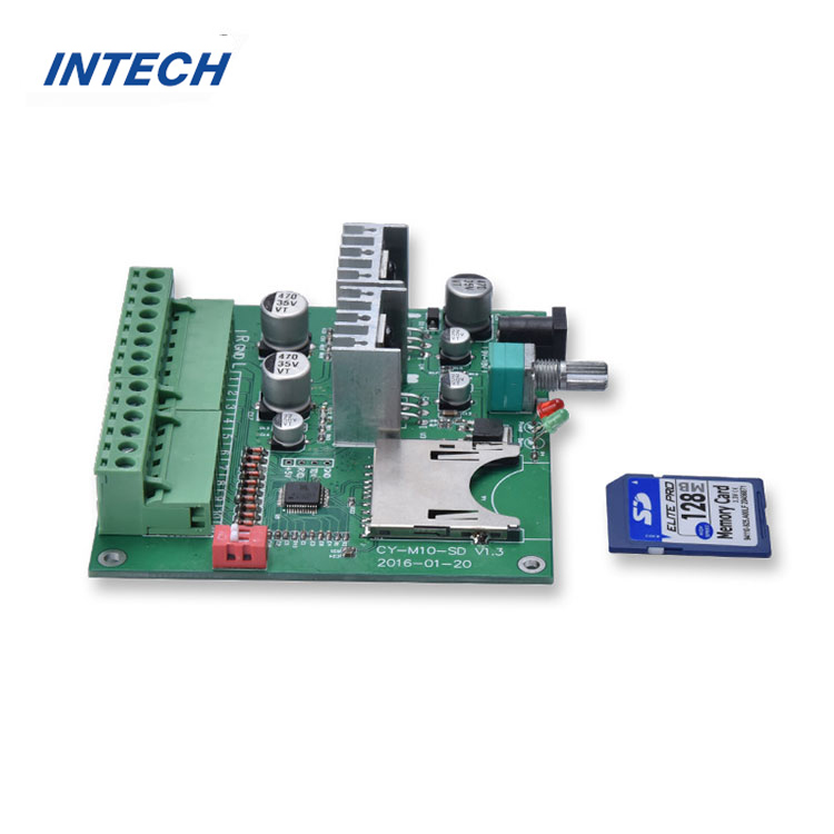
How to test after assembled pcb board?
Date:2023-12-25 16:29:19
Assembled PCB boards are an integral part of electronic devices, ensuring their proper functioning and reliability. Thus, it is crucial to test these boards thoroughly before deploying them in real-world applications. This article outlines various testing methods and techniques to ensure the quality and performance of assembled PCB boards.
1. Visual Inspection
Visual inspection is the initial step in testing assembled PCB boards. It involves carefully examining the board for any physical defects, such as misalignment, solder bridges, component damage, or missing components. This inspection can be performed manually or using automated optical inspection (AOI) systems. Visual inspection helps to identify and rectify manufacturing defects early in the process.
2. In-Circuit Testing (ICT)
In-circuit testing is a popular method for evaluating the functionality of individual components and connections on an assembled PCB board. It involves the use of specialized test probes that make contact with specific points on the board to measure voltages, currents, and resistances. ICT helps in identifying open or short circuits, component values, and manufacturing defects such as reversed components or incorrect polarity.
3. Automated Functional Testing
Automated functional testing is performed to verify the overall performance of the assembled PCB board. This testing involves the use of specialized test fixtures and software that simulate real-world operating conditions and input signals. The board is subjected to a series of predefined tests to ensure its functions, interfaces, and features work as intended. Automated functional testing offers a comprehensive evaluation of the board's capabilities.
4. Boundary Scan Testing
Boundary scan testing, also known as JTAG testing, is a technique used to assess the interconnectivity and functionality of digital components on a PCB board. It employs the JTAG (Joint Test Action Group) standard, which allows for the testing of chips with JTAG support. Boundary scan testing helps identify faults in signal paths, shorts, open circuits, and verifies the correct operation of integrated circuits.

5. Environmental Testing
Environmental testing is essential to ensure the reliability and performance of PCB boards under various operating conditions. This includes subjecting the boards to temperature extremes, humidity, vibrations, and electrical stress. Environmental testing helps identify any issues related to thermal management, mechanical stability, and electrical robustness. It ensures the board's performance in real-world scenarios.
6. X-ray Inspection
X-ray inspection is a non-destructive testing method used to examine the internal structure of the assembled PCB board. By using X-rays, it allows for the detection of hidden defects, such as solder joint quality, shorts, or open circuits, without physically damaging the board. X-ray inspection is particularly useful for complex designs with high-density components.
7. Burn-in Testing
Burn-in testing involves subjecting assembled PCB boards to prolonged stress by applying power and operational loads. This stress test helps identify latent defects or failures that may occur during extended usage. Burn-in testing is especially critical for sensitive components and high-reliability applications, ensuring the board's stability and longevity.
Conclusion
Thorough testing of assembled PCB boards is essential to ensure their quality, reliability, and performance. From visual inspection to burn-in testing, employing a comprehensive testing approach helps identify and rectify any manufacturing defects or functional abnormalities. By following these testing methods, manufacturers can ensure that the assembled PCB boards meet the required standards and provide optimal performance in diverse electronic applications.
