 English
Package and Layout Optimization in PCB Design
Date:2023-06-20 17:25:28
Packaging and layout optimization in PCB design PCB (Printed Circuit Board, printed circuit board) is an indispensable part of modern electronic equipment. In the PCB design process, packaging and layout optimization are crucial links. This article will introduce the importance of package and layout optimization in PCB design, and provide some practical tips and suggestions.
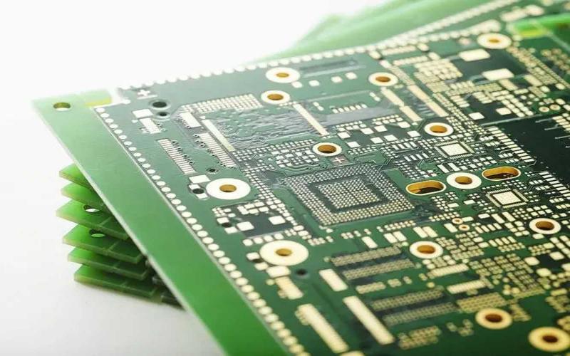
First of all, packaging refers to packaging electronic components (such as chips, resistors, capacitors, etc.) into a standard size and shape for easy layout and soldering on the PCB. Choosing the right package is critical to circuit performance and reliability. When choosing a package, factors such as the component's power dissipation, thermal requirements, size constraints, and interconnections to other components need to be considered. Generally speaking, common package types include DIP (Dual In-line Package), SMD (Surface Mount Device) and BGA (Ball Grid Array). Different package types have different characteristics and applicable scenarios, and designers need to choose according to specific needs.
Second, layout optimization refers to rationally arranging the location and interconnection paths of electronic components on the PCB to maximize circuit performance and reliability. The goal of layout optimization is to minimize signal transmission paths, reduce interference and noise, while ensuring good thermal distribution and heat dissipation between components. When laying out, factors such as signal integrity, power supply distribution, ground wire planning, and heat dissipation design need to be considered. Here are some practical tips for layout optimization:
1. Layered layout: divide the circuit board into different layers, and separate the signal layer, power layer and ground layer to reduce signal interference and improve power stability.
2. Signal integrity: Separate high-speed signal lines and low-speed signal lines to avoid mutual interference. Use differential signal line layout to improve anti-interference ability.
3. Thermal management: Reasonably arrange the position of heat dissipation components (such as heat sinks, heat dissipation holes, etc.) to ensure good heat dissipation of components and avoid performance degradation or damage caused by overheating.
4. Component spacing: Arrange the spacing between components reasonably to facilitate welding and maintenance. Avoid overcrowding between components, so as not to affect the convenience of heat dissipation and maintenance.
5. Power supply planning: rationally layout power lines to ensure the stability and reliability of power supply. Avoid crossing power lines and signal lines to reduce interference.
Layout optimization also needs to take into account the feasibility of manufacturing and assembly. When doing layout, it is necessary to communicate with the PCB manufacturer and assembler to understand their requirements and constraints to ensure the manufacturability and assembly of the design.
In summary, package and layout optimization in PCB design is critical to circuit performance and reliability. By choosing a suitable package and rationally optimizing the layout, the working efficiency of the circuit can be improved, interference and failure can be reduced, and the quality and reliability of the overall product can be improved. Designers should continue to learn and master relevant knowledge and skills to improve their ability and level in the field of PCB design.
